

-
Profile
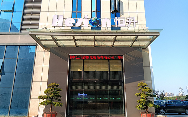
Hesion is proud to have clients like you, and we will do our best to provide you with excellent service and become your loyal partner and friend!
-
Product
TENS electrode film; conductive carbon film; PE conductive film; anti-static shielding film; anti-static film; anti-static shielding bag; anti-static bag; conductive bag; conductive grid bag; automatic packaging bag; PET anti-static film; conductive tape; plastic packaging; anti-static plastic; transparent conductive sheet; anti-static plastic stationery.
-

Cases
Functional films; shielding materials; plastic sheets; anti-static conductive plastic films; electronic product packaging; plastic packaging products.

News
Aggregate industry real-time dynamics and release news information. Welcome your attention.
Innovative Uses of ESD Wafer Separation Film in High-Tech Industries
Release Time:
2025.11.07
Innovative Uses of ESD Wafer Separation Film in High-Tech Industries
Table of Contents
- 1. Introduction to ESD Wafer Separation Film
- 2. What is ESD Wafer Separation Film?
- 3. Importance of ESD Wafer Separation Film in High-Tech Industries
- 4. Applications of ESD Wafer Separation Film
- 4.1 In the Semiconductor Industry
- 4.2 In Solar Cell Manufacturing
- 4.3 In Electronics Manufacturing
- 4.4 In Advanced Packaging Techniques
- 5. Benefits of Using ESD Wafer Separation Film
- 6. Future Trends in ESD Wafer Separation Film
- 7. Frequently Asked Questions
- 8. Conclusion
1. Introduction to ESD Wafer Separation Film
In the rapidly evolving landscape of high-tech industries, the demand for innovative materials that enhance production efficiency and product quality is paramount. One such material is **Electrostatic Discharge (ESD) wafer separation film**. This specialized film plays a crucial role in safeguarding sensitive electronic components during manufacturing processes.
As we delve into the innovative uses of ESD wafer separation film, we will explore its significance, applications, and the benefits it brings to various high-tech sectors.
2. What is ESD Wafer Separation Film?
ESD wafer separation film is a type of protective film designed to prevent electrostatic discharge during the handling and processing of wafers in semiconductor and electronic manufacturing. It acts as a barrier that minimizes the risk of contamination and damage to wafers, which are critical components in the production of integrated circuits and other electronic devices.
Typically made from advanced polymer materials, ESD films are engineered to have specific properties, including:
- **High transparency** for optimal visibility.
- **Durability** to withstand the rigors of various manufacturing processes.
- **Low static charge generation** to prevent damage to sensitive electronic components.
3. Importance of ESD Wafer Separation Film in High-Tech Industries
The significance of ESD wafer separation film in high-tech industries cannot be overstated. As the demand for smaller, faster, and more efficient electronic devices continues to grow, manufacturers are under increased pressure to ensure that their production processes are not only efficient but also safe.
**Key reasons for its importance include:**
- **Protection Against Electrostatic Discharge:** ESD film prevents the accumulation of static electricity, which can lead to catastrophic failures in sensitive components.
- **Improved Yield Rates:** By protecting wafers during processing, manufacturers can achieve higher yield rates and reduce waste.
- **Enhancing Product Quality:** The use of ESD films leads to fewer defects, resulting in higher quality end products.
4. Applications of ESD Wafer Separation Film
The versatility of ESD wafer separation film allows its application across various high-tech industries. Below are some of the most prominent applications:
4.1 In the Semiconductor Industry
In the semiconductor industry, ESD wafer separation film serves as a vital component in the manufacturing process, particularly during wafer handling and transport. The film is used to:
- **Protect wafers from contamination** during processing.
- **Facilitate efficient handling** of sensitive materials in cleanroom environments.
- **Ensure compatibility with automated equipment**, enhancing overall production efficiency.
4.2 In Solar Cell Manufacturing
The solar cell manufacturing process benefits significantly from ESD wafer separation film. It helps to:
- **Prevent damage to cells** during the assembly and testing phases.
- **Maintain the integrity of photovoltaic materials**, thus improving energy conversion efficiency.
- **Ensure safe transport** of solar cells to different manufacturing stages.
4.3 In Electronics Manufacturing
In electronics manufacturing, ESD films are crucial for protecting various components, including:
- **Microprocessors** and **memory chips**, which are highly sensitive to electrostatic discharge.
- **Surface mount devices (SMDs)** during assembly processes, minimizing the risk of failure.
4.4 In Advanced Packaging Techniques
Advanced packaging techniques, such as System in Package (SiP) and 3D packaging, rely on ESD wafer separation film to:
- **Facilitate precise alignment** of components, ensuring optimal performance.
- **Protect intricate circuits** during assembly, leading to enhanced durability and reliability.
5. Benefits of Using ESD Wafer Separation Film
The adoption of ESD wafer separation film brings numerous benefits to manufacturers:
- **Cost Efficiency:** By reducing defects and improving yield rates, companies can save significant costs associated with rework and scrap materials.
- **Enhanced Product Lifespan:** The protective qualities of ESD films contribute to longer product life cycles, ensuring that devices remain functional and reliable.
- **Regulatory Compliance:** Utilizing ESD films can help manufacturers meet stringent industry standards and regulations, particularly in sensitive sectors like aerospace and medical electronics.
- **Environmental Impact:** ESD films can be recycled or disposed of safely, contributing to more sustainable manufacturing practices.
6. Future Trends in ESD Wafer Separation Film
As technology continues to advance, the future of ESD wafer separation film looks promising. Emerging trends include:
- **Smart Materials:** Incorporating smart technology into ESD films that can monitor static levels in real-time, providing manufacturers with valuable data for process optimization.
- **Biodegradable Options:** The development of eco-friendly ESD films that minimize environmental impact while maintaining performance standards.
- **Customization:** Increasing demand for tailored solutions that meet specific industry requirements, leading to more specialized ESD film products.
7. Frequently Asked Questions
**Q1: What materials are used to make ESD wafer separation film?**
A1: ESD wafer separation films are typically made from specialized polymer materials designed to provide static protection and physical durability.
**Q2: How does ESD wafer separation film prevent damage to wafers?**
A2: The film acts as a barrier that dissipates static charges, preventing electrostatic discharge that can harm sensitive electronic components.
**Q3: Can ESD wafer separation film be reused?**
A3: While some ESD films may be designed for reuse, it is generally recommended to use new film for optimal protection and performance.
**Q4: What industries benefit the most from ESD wafer separation film?**
A4: The semiconductor, solar cell manufacturing, electronics, and advanced packaging industries are among the primary sectors that benefit from ESD wafer separation film.
**Q5: How can manufacturers ensure they select the right ESD film for their needs?**
A5: Manufacturers should consider factors such as thickness, transparency, and static dissipative properties when selecting ESD wafer separation film.
8. Conclusion
In conclusion, **ESD wafer separation film** is an essential material in high-tech industries, offering robust protection against electrostatic discharge while enhancing production efficiency and product quality. Its diverse applications across semiconductor, solar cell, and electronics manufacturing underline its vital role in modern production processes.
As technology continues to evolve, the future of ESD films looks bright, with innovations on the horizon promising even greater benefits. By understanding and leveraging the capabilities of ESD wafer separation film, manufacturers can stay ahead in the competitive high-tech landscape, ensuring that they produce reliable and high-quality electronic components.
Let's stay in touch!
We provide you with standardized products, develop customized products, and provide solutions to meet the diverse needs of customers
Service Hotline
Inquire Now
Company Address: No. 691, Huanchang North Road, Changping Town, Dongguan City, Guangdong Province, Building 1, Floor 1, Shangshang Industrial Park
Email:hesion@foxmail.com


WeChat Official Account
Alibaba Credit Pass
Copyright of this page belongs to Dongguan Hesion Anti-static Products Co., Ltd.
Website:300.cn dongguan.300.cn SEO Privacy Policy