

-
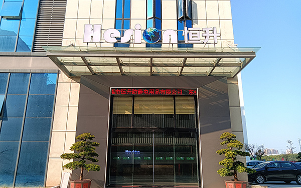
Profile
Hesion is proud to have clients like you, and we will do our best to provide you with excellent service and become your loyal partner and friend!
-
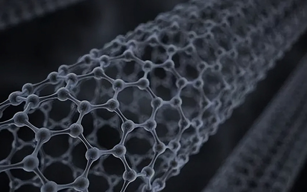
Product
TENS electrode film; conductive carbon film; PE conductive film; anti-static shielding film; anti-static film; anti-static shielding bag; anti-static bag; conductive bag; conductive grid bag; automatic packaging bag; PET anti-static film; conductive tape; plastic packaging; anti-static plastic; transparent conductive sheet; anti-static plastic stationery.
-

Cases
Functional films; shielding materials; plastic sheets; anti-static conductive plastic films; electronic product packaging; plastic packaging products.

News
Aggregate industry real-time dynamics and release news information. Welcome your attention.
The Evolution of ESD Wafer Separation Film in Modern Industry
Release Time:
2026.09.24
The Evolution of ESD Wafer Separation Film in Modern Industry
Table of Contents
- 1. Introduction to ESD Wafer Separation Film
- 2. Understanding ESD (Electrostatic Discharge) and Its Importance
- 3. Historical Development of ESD Wafer Separation Film
- 4. Material Innovations in ESD Wafer Separation Film
- 5. Applications of ESD Wafer Separation Film in Modern Industry
- 6. Benefits and Advantages of ESD Wafer Separation Film
- 7. Future Trends in ESD Wafer Separation Film Development
- 8. Frequently Asked Questions
- 9. Conclusion
1. Introduction to ESD Wafer Separation Film
In the modern landscape of semiconductor manufacturing, **Electrostatic Discharge (ESD)** poses significant risks to sensitive electronic components. As the demand for advanced technology escalates, so does the need for effective protective measures. This is where **ESD wafer separation film** comes into play. It is a specialized material designed to provide a buffer against electrostatic discharge, ensuring the integrity of wafers during the manufacturing process. This article explores the evolution, innovations, applications, and future trends of ESD wafer separation film, emphasizing its critical role in modern industry.
2. Understanding ESD (Electrostatic Discharge) and Its Importance
Electrostatic discharge occurs when there is a sudden flow of electricity between two objects with different electrical charges. This phenomenon can lead to severe damage in semiconductor devices, causing performance degradation or complete failure. Understanding the significance of ESD is crucial for manufacturers aiming to protect their products and maintain quality.
2.1 The Impact of ESD on Semiconductor Manufacturing
The semiconductor industry is particularly vulnerable to ESD, given the delicate nature of the components involved. A single discharge can destroy sensitive circuits and result in costly downtimes. Consequently, manufacturers are compelled to implement robust ESD protection measures throughout the production process.
2.2 Regulatory Standards for ESD Protection
Various regulatory bodies have established stringent guidelines for ESD control in manufacturing settings. Compliance with these standards is essential not only for product quality but also for ensuring safety and reliability in electronic devices.
3. Historical Development of ESD Wafer Separation Film
The genesis of ESD wafer separation film can be traced back to the increasing complexity and miniaturization of electronic components. Early attempts to mitigate ESD-related risks included rudimentary protective measures, but as technology advanced, so did the sophistication of the materials used.
3.1 The Early Days of ESD Protection
In the initial stages, manufacturers relied on basic insulating materials that failed to address the nuanced requirements of ESD protection. As the industry evolved, there was a clear need for specialized films that could offer enhanced performance.
3.2 The Introduction of ESD Wafer Separation Film
The introduction of ESD wafer separation film marked a turning point in the industry. This film was engineered to provide superior protection while maintaining the delicate balance required for wafer handling. Early iterations were primarily focused on static dissipative properties, but advancements have led to films with multi-functional capabilities.
4. Material Innovations in ESD Wafer Separation Film
The quest for better ESD wafer separation films has driven significant innovations in material science. These advancements have resulted in films that not only protect against electrostatic discharge but also exhibit other desirable properties.
4.1 Conductive Polymer Films
Conductive polymers have emerged as a game-changer in the production of ESD wafer separation films. By incorporating conductive elements, these films provide enhanced static dissipative properties, ensuring that any accumulated charge is safely redirected.
4.2 Advanced Coatings and Treatments
Innovative coatings and treatments have been developed to enhance the performance of ESD wafer separation films. These include anti-static coatings, which further prevent the buildup of static electricity and improve the overall efficacy of the film.
4.3 Biodegradable Options
With growing environmental concerns, the industry is also exploring biodegradable materials for ESD wafer separation films. This movement not only addresses ecological sustainability but also meets the demands of a more environmentally conscious market.
5. Applications of ESD Wafer Separation Film in Modern Industry
The application of ESD wafer separation film extends beyond just semiconductor manufacturing. Its versatility has led to its adoption in various sectors where ESD protection is paramount.
5.1 Semiconductor Manufacturing
In semiconductor manufacturing, ESD wafer separation films are crucial for protecting wafers during processing and transport. They help minimize the risk of electrostatic discharge, ensuring yield and quality.
5.2 Electronics Assembly
In electronics assembly, these films play a vital role in safeguarding components from ESD damage during assembly and packaging, contributing to the overall reliability of the final product.
5.3 Medical Devices
As medical devices become more integrated with advanced electronics, the need for robust ESD protection has increased. ESD wafer separation films are now used to protect sensitive components in devices such as pacemakers and diagnostic equipment.
5.4 Automotive Sector
The automotive industry has also recognized the importance of ESD protection, particularly with the rise of electric vehicles and advanced driver-assistance systems (ADAS). ESD wafer separation films help protect the sensitive electronics involved in these technologies.
6. Benefits and Advantages of ESD Wafer Separation Film
The advantages of ESD wafer separation film extend across various dimensions, making it an essential component in modern manufacturing processes.
6.1 Enhanced Protection Against ESD
The primary benefit of ESD wafer separation film is its ability to provide robust protection against electrostatic discharge, reducing the risk of damage to sensitive components.
6.2 Improved Manufacturing Efficiency
By minimizing ESD-related failures, manufacturers can achieve higher efficiency and productivity. This leads to reduced downtime and lower costs associated with defective products.
6.3 Versatility and Adaptability
ESD wafer separation films are adaptable and can be customized to meet specific requirements across different industries. This versatility ensures that manufacturers can find solutions tailored to their unique needs.
6.4 Environmental Benefits
With the advent of biodegradable options, ESD wafer separation films can contribute to sustainability efforts within manufacturing processes, aligning with global goals for environmental responsibility.
7. Future Trends in ESD Wafer Separation Film Development
As technology continues to evolve, so too will the development of ESD wafer separation films. Several emerging trends are likely to shape the future of this critical component.
7.1 Integration with Smart Technologies
The integration of smart technologies, such as Internet of Things (IoT) devices, is expected to drive demand for enhanced ESD protection. Manufacturers will seek advanced films that can accommodate the increased complexity of modern electronics.
7.2 Focus on Sustainability
As environmental concerns continue to grow, the push for sustainable materials will significantly influence the future of ESD wafer separation film development. We can expect to see more environmentally friendly options entering the market.
7.3 Advances in Nanotechnology
The application of nanotechnology in the development of ESD wafer separation films is an exciting frontier. Nanomaterials can enhance the performance of films, leading to improved protection and functionality.
8. Frequently Asked Questions
8.1 What is ESD wafer separation film?
ESD wafer separation film is a specialized material designed to protect semiconductor wafers from electrostatic discharge during manufacturing processes.
8.2 How does ESD wafer separation film work?
It works by dissipating static electricity, preventing the buildup of electrostatic charges that can damage sensitive electronic components.
8.3 What industries use ESD wafer separation film?
ESD wafer separation film is primarily used in semiconductor manufacturing but is also utilized in electronics assembly, medical devices, and the automotive sector.
8.4 Are there biodegradable options available for ESD wafer separation film?
Yes, the industry is exploring biodegradable materials for ESD wafer separation films to promote environmental sustainability.
8.5 What are the benefits of using ESD wafer separation film?
The benefits include enhanced protection against ESD, improved manufacturing efficiency, versatility across industries, and potential environmental benefits.
9. Conclusion
The evolution of ESD wafer separation film is a testament to the ongoing advancements in material science and technology. As industries continue to prioritize the protection of sensitive electronic components, the demand for effective ESD solutions will only grow. By understanding the importance of ESD wafer separation film and embracing innovations, manufacturers can safeguard their products, enhance efficiency, and contribute to a more sustainable future. As we move forward, the future of ESD wafer separation film promises exciting developments that will further revolutionize the industry.
Recommended Dynamics
Let's stay in touch!
We provide you with standardized products, develop customized products, and provide solutions to meet the diverse needs of customers
Service Hotline
Inquire Now
Company Address: No. 691, Huanchang North Road, Changping Town, Dongguan City, Guangdong Province, Building 1, Floor 1, Shangshang Industrial Park
Email:hesion@foxmail.com


WeChat Official Account
Alibaba Credit Pass
Copyright of this page belongs to Dongguan Hesion Anti-static Products Co., Ltd.
Website:300.cn dongguan.300.cn SEO Privacy Policy